Table of Content
It's not absolutely necessary to read this section to understand the rest of the article. The Interposer board, soldered on the Google Home Mini PCB, ready to be used. These evenly spaced and sized solder balls will help greatly when it comes to solder the Interposer to the Google Home PCB. To help with the soldering process, I ordered a stencil at the same time with the Interposer PCB. The holes of the stencil are matching the NAND Flash footprint.
This source code will be extremely useful in the second article of this series. In 2014, fail0verflow was able to root Chromecast devices with a vulnerability affecting the bootloader. A buffer overflow vulnerability triggered thanks to a special USB peripheral led to a full secure boot bypass. That said, the Home Mini used a micro-USB port instead of a barrel plug connector, and some people preferred that approach.
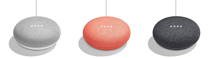
Google Home Mini
You can access all of the recordings through your Google account and even turn off recording, although that does prevent some Google Home features from working. While all the executable data is apparently verified, having a total control on all the NAND Flash data does open a rather large attack surface. In order to mount and eventually alter the content of these partitions, I choose to use the exact same YAFFS2 driver that can be found on Google's shared files. The simple file utility can be used against this image to reveal it's in fact a Squashfs filesystem. Please note the Kernel version, sources, initramfs and init.rc file will be useful in the second part of this series of article.
” to get answers to the most common privacy and security questions. Its in-store longevity could have been due to Google making too many at launch, and you will undoubtedly find a handful on store shelves if you still really want one. That said, the Home Mini does not appear on Best Buy or Target online stores today.
Google Home Mini Hardware Overview
However, looking at the Flash datasheet, it appears the maximum speed was not that fast, and I chose to take the risk. I personally find this combination of a FT2232H and ICE40HX1K-TQ144 to be quite interesting and versatile. However, please note that using both the SPI mode and Synchronous FIFO mode of the FT2232H requires adding a EEPROM to the BOM. This EEPROM contains configuration data for the FT2232H and can sometimes be omitted.
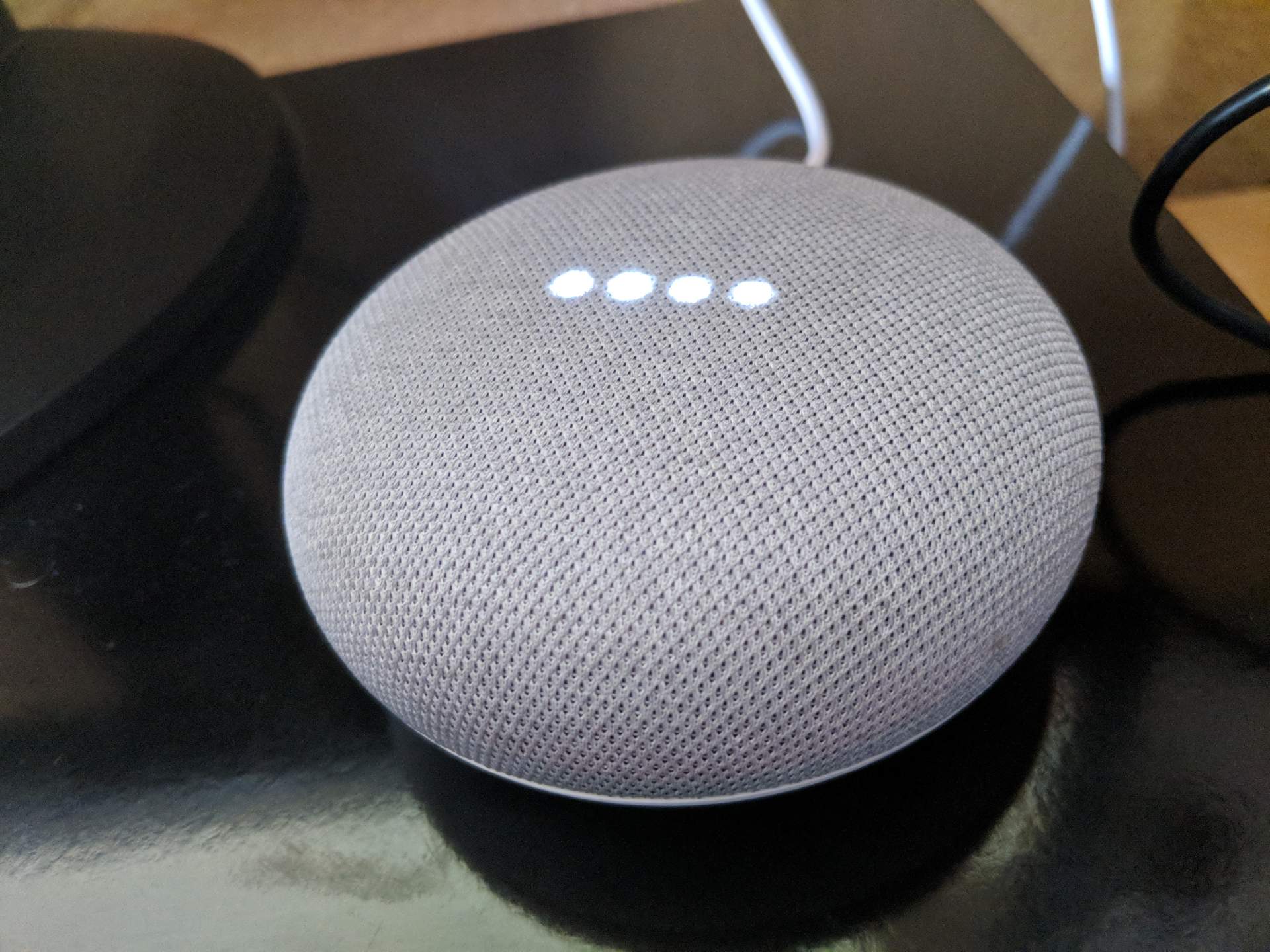
Unlike the Home Mini, the Nest Mini comes with a built-in wall mount. It also provides better sound, with improved bass response, although the physical speakers in both devices use 40mm drivers. If you already have one or more Google Home devices, then the Home Mini is a great way to extend the same functionality you're familiar with into every room in your house. Since the Google Home Mini has all of the same functionality as the Google Home, it makes a good entry-level smart speaker. Like all Google Home devices, the Home Mini is built around the Google Assistant virtual assistant, so it is operated almost entirely via voice commands. It listens for a wake word, which is "Okay, Google," and then records anything it hears after the wake word.
Google Nest Mini (thế hệ Loa thông minh tích hợp trợ lý Google
Using strings and grep against the firmware dump can quickly reveal interesting bits of information. It was now time to actually have a look at the content of the NAND Flash dump. Playing with the bchlib Python library somewhat confirmed this hypothesis. The length of the ECC data we measured thanks to the graphical visualization could match a BCH-48 algorithm. A glance at the bootloader/berlin_tools/bootloader/nand_ctrl/mv_nand.c file is enough to understand the ECC is calculated by the hardware of the main SoC itself.
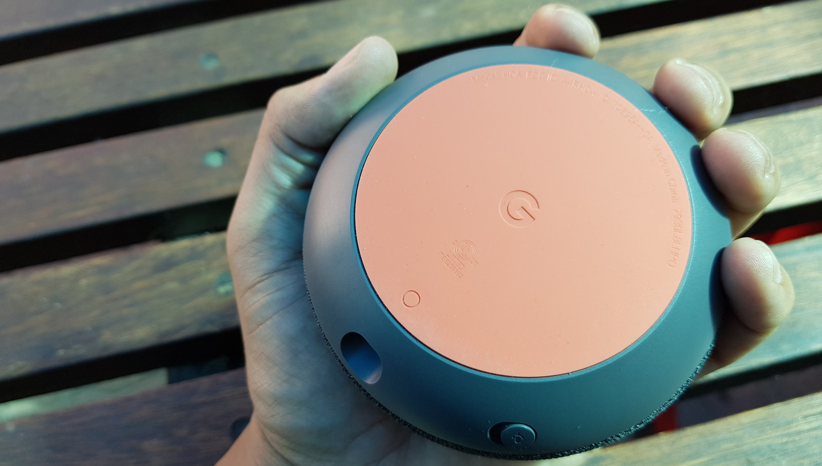
The delicate BGA NAND Flash IC is soldered to this board. As explained before, the SoC of the Google Home Mini comes without any public documentation. Being able to run custom code on it is valuable to understand it better. Things like dumping the BootROM of the system becomes possible.
More on Google Home:
The Google Home Mini is a smart speaker that's built on the same platform as the original Google Home, but it's significantly smaller. If the device has been used before, factory reset your speaker or display before you continue. The Google Home has a single speaker with two passive radiators, which really help it produce decent sound for a device of its size.

However, The NAND Flash signals are going too fast for achieving this with a simple ICE40 FPGA. This may have been possible with a more advance component. This script will simply generate the Passthrough bitstream and upload it to the FPGA. To generate the needed SPI and GPIO signals, the FT2232H is used in MPSSE Mode.
Just start with “Hey Google” to get answers from your Google Assistant, tackle your day, enjoy music or TV shows, and control your compatible smart home devices. And with Voice Match, the Assistant can tell your voice from others—up to six people can get personal assistance on each device. If you want to set up a different device, you can find the instructions in Set up smart devices in the Google Home app.

The Google Home app is designed to show you the status of your home and keep you up to date with what you may have missed. Check in on your home anytime and see a recap of recent events. You can also get a notification if something important happens while you’re away. Turn on the lights, adjust the thermostat, or get an alert when there’s a person or package at your front door. Google Home on WearOS will be available as a preview as we continue to add controls and improvements.
The Google Home Mini PCB + Interposer Board can be connected to the NandBug Main Board. As it must be soldered like a BGA component, I'll turn it into one by soldering tiny solder balls. First things first, the NAND Flash must be desoldered from the Google Home PCB. This has been done with a cheap hot air reworking station. It's a model that can be bought from many places and that has served me well for several years now. A small connector matching the one of the main board.


No comments:
Post a Comment