Table of Content
It's a mirrored version of the "normal" NAND Flash schematic. Indeed, this board will be soldered in place of the original NAND on the Google Home Mini PCB. Sending various configuration bitstreams to the FPGA. This is done by using the SPI protocol and a couple of additional GPIOs. Manually soldering thin wires to the BGA footprint for breaking out the NAND Flash lines could have been risky because of signal integrity issues. It wouldn't have been a very clean and, more importantly, reliable solution.

The Google Home Mini PCB + Interposer Board can be connected to the NandBug Main Board. As it must be soldered like a BGA component, I'll turn it into one by soldering tiny solder balls. First things first, the NAND Flash must be desoldered from the Google Home PCB. This has been done with a cheap hot air reworking station. It's a model that can be bought from many places and that has served me well for several years now. A small connector matching the one of the main board.
More by Google LLC
Optionally, a NAND Flash can be directly soldered to the board. A FT2232H. This component adds Hi-Speed USB connectivity to the board. Hardware files are available here while the software can be downloaded from here. I made the schematics, Gerber files, and software of NandBug publicly available. The general idea is in fact to make the NAND Flash of the Google Home in-system programmable. It may sound like an over engineered solution and it maybe is.
Another transformation was applied to the data before or after BCH encoding. However, this information alone isn't enough to compute the ECC in the exact same way with the hardware. Each page is very likely using an ECC placed in the OOB area. Further, for two identical "data" pages, the corresponding OOB area will be the same as well. Given this information, a graphical representation of the binary dumped data can quickly help checking whether the OOB section is likely to be used for storing ECC or not.
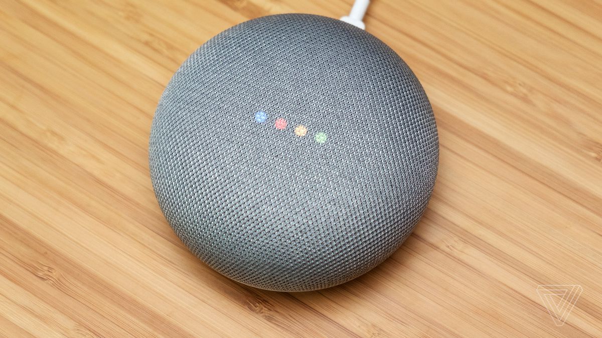
What Is a Google Home Mini and How Does It Work?
” to get answers to the most common privacy and security questions. Its in-store longevity could have been due to Google making too many at launch, and you will undoubtedly find a handful on store shelves if you still really want one. That said, the Home Mini does not appear on Best Buy or Target online stores today.

On the bottom side of the board, only the Interposer Board connector is fitted. Its bitstream format has been reverse-engineered and it is now supported by open source toolchains. A micro-USB connector, used for power and data transfer.
The NandBug System
The delicate BGA NAND Flash IC is soldered to this board. As explained before, the SoC of the Google Home Mini comes without any public documentation. Being able to run custom code on it is valuable to understand it better. Things like dumping the BootROM of the system becomes possible.

Set up your Nest Wifi and Google Wifi in minutes using the Google Home app. Run speed tests, set up a guest network, and easily share your Wi-Fi password with family and friends. Use parental controls like Wi-Fi pause to manage online time for the kids. Automatically prioritize video conferencing and gaming traffic on all devices, or decide which devices to prioritize for all traffic types. Get more insights on your network, whether it’s a notification when a new device joins your network or detailed insights for troubleshooting a poor internet connection. The Google Home app will walk you through the steps to set up your Google Nest or Home speaker or display.
It's not absolutely necessary to read this section to understand the rest of the article. The Interposer board, soldered on the Google Home Mini PCB, ready to be used. These evenly spaced and sized solder balls will help greatly when it comes to solder the Interposer to the Google Home PCB. To help with the soldering process, I ordered a stencil at the same time with the Interposer PCB. The holes of the stencil are matching the NAND Flash footprint.
For unidirectional signals, this connection can be achieved directly. However, for the bidirectional signals of the data bus, some arbitration is needed. In this mode, the FPGA will directly connect all the NAND Flash signals between the Google Home circuit and the NAND Flash. Here again, the FPGA is directly clocked by the 60MHz signal generated by the FT2232H when it's used in this mode. The FPGA is directly clocked by the 60MHz signal generated by the FT2232H when it's used in this mode. I do find these two languages rather annoying to use.
The first thing to note is that the way the data is written to a NAND Flash is somewhat special. Each page contains data and a special section called OOB, the out-of-bound section. This feature can somehow work a little bit at the very beginning of the Google Home boot sequence though. A this early point, the clock of the NAND Flash peripheral is reduced to a couple of hundred of kHz. More importantly, the Google Home Mini can still boot without problems despite all the heavy surgery it received. Receive the NAND Flash data and compare it to the content of filename.

The NAND Flash hardware peripheral of the processor is fully responsible from computing it. The only hint the source can give is that the ECC algorithm in use is very likely BCH. It's needed to correct the dump and to go further with unpacking the firmware files.
Dynamic analysis of the Goggle Home software running on the actual hardware becomes possible. While extremely informative, the attack described by the presentation cannot be used against my own device anymore. The acoustic hole is on the other side of the PCB. Some RF shields have been removed to expose the components.

Safety starts with understanding how developers collect and share your data. Data privacy and security practices may vary based on your use, region, and age. The developer provided this information and may update it over time. Protecting your privacy starts with one of the world’s most advanced security infrastructures, which we build directly into Google products so that they’re secure by default. The built-in security in your Google Account automatically detects and blocks threats before they reach you, so that your personal information is secure.
Finally, it's important to note that the main CPU comes without public documentation. Very few details about this component are available online. All the juicy technical data is likely protected by a NDA. The main speaker of the Google Home can be plugged to this two pins connector. Visit the Google Nest Safety Center at safety.google/nest to learn more about how we protect your information and respect your privacy. Control your Google Assistant activity, privacy settings, information, and personal preferences.


No comments:
Post a Comment